How to Design Electronic Packaging for Maximum Protection
Developing packaging for electronics isn’t the same as designing for general consumer goods. Electronic components introduce a mix of fragility, precision, and regulatory obligations that make packaging performance non-negotiable. Screens need protection without pressure points. Ports and buttons can’t be stressed. Retailers expect clean presentation and consistent sealing. And every detail must survive transportation, handling, and the realities of high-volume fulfillment.
Successful electronics packaging depends on aligning design, forming feasibility, and protection needs early, well before tooling is cut. When engineering teams and packaging partners collaborate upfront, you avoid redesign loops, eliminate unmanufacturable geometry, and ensure the packaging performs reliably from prototype through production.
Understanding the Protection Requirements for Electronic Packaging
Every electronic product has unique vulnerabilities, and those should drive the packaging strategy before any design decisions. A strong process starts by defining what needs protection, from what hazards, and under which conditions.
Key considerations include:
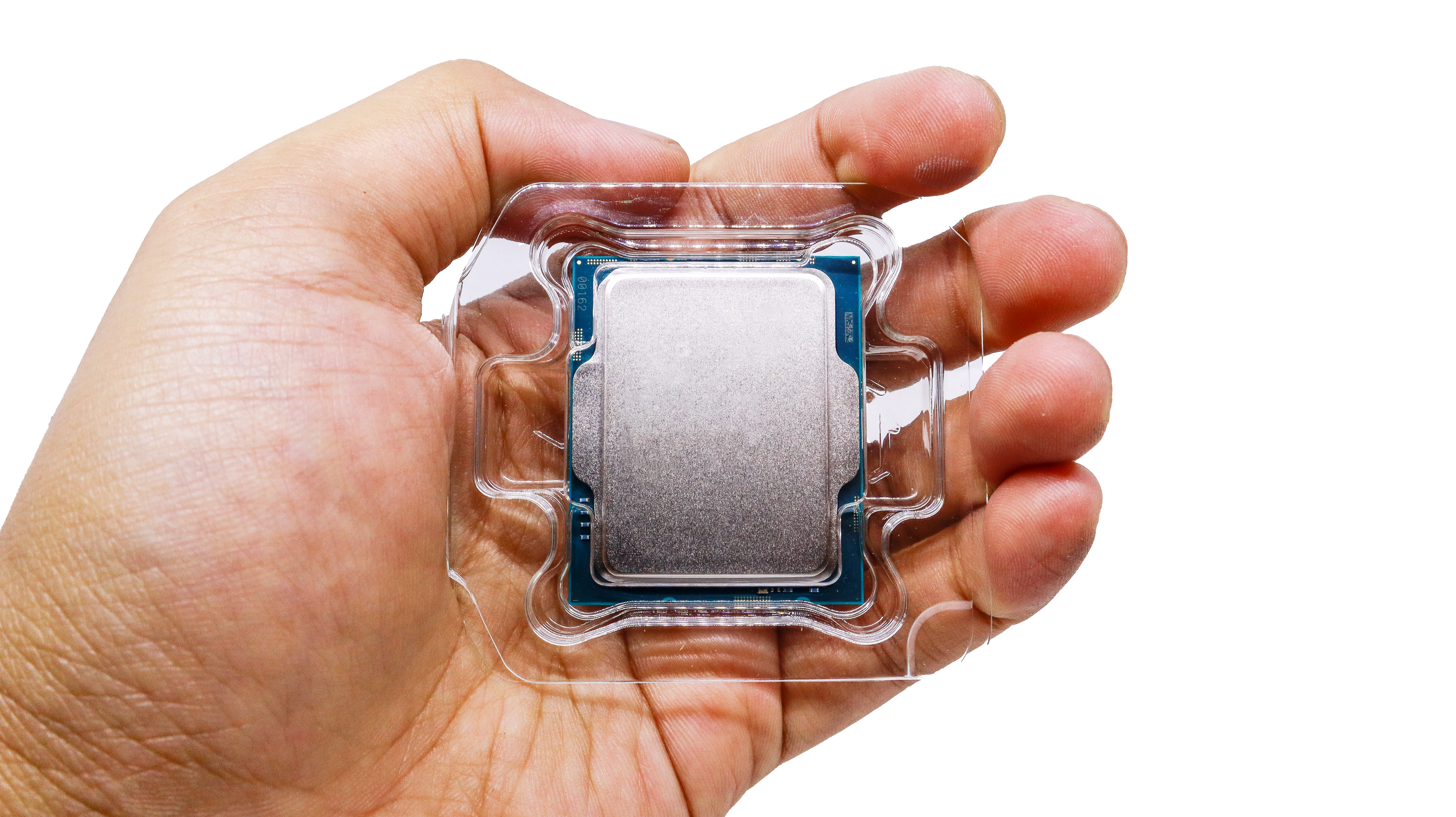
Static sensitivity: Even a small electrostatic discharge can damage sensors, boards, and microchips. Selecting the right ESD-safe material early prevents failures during assembly, transport, or use.
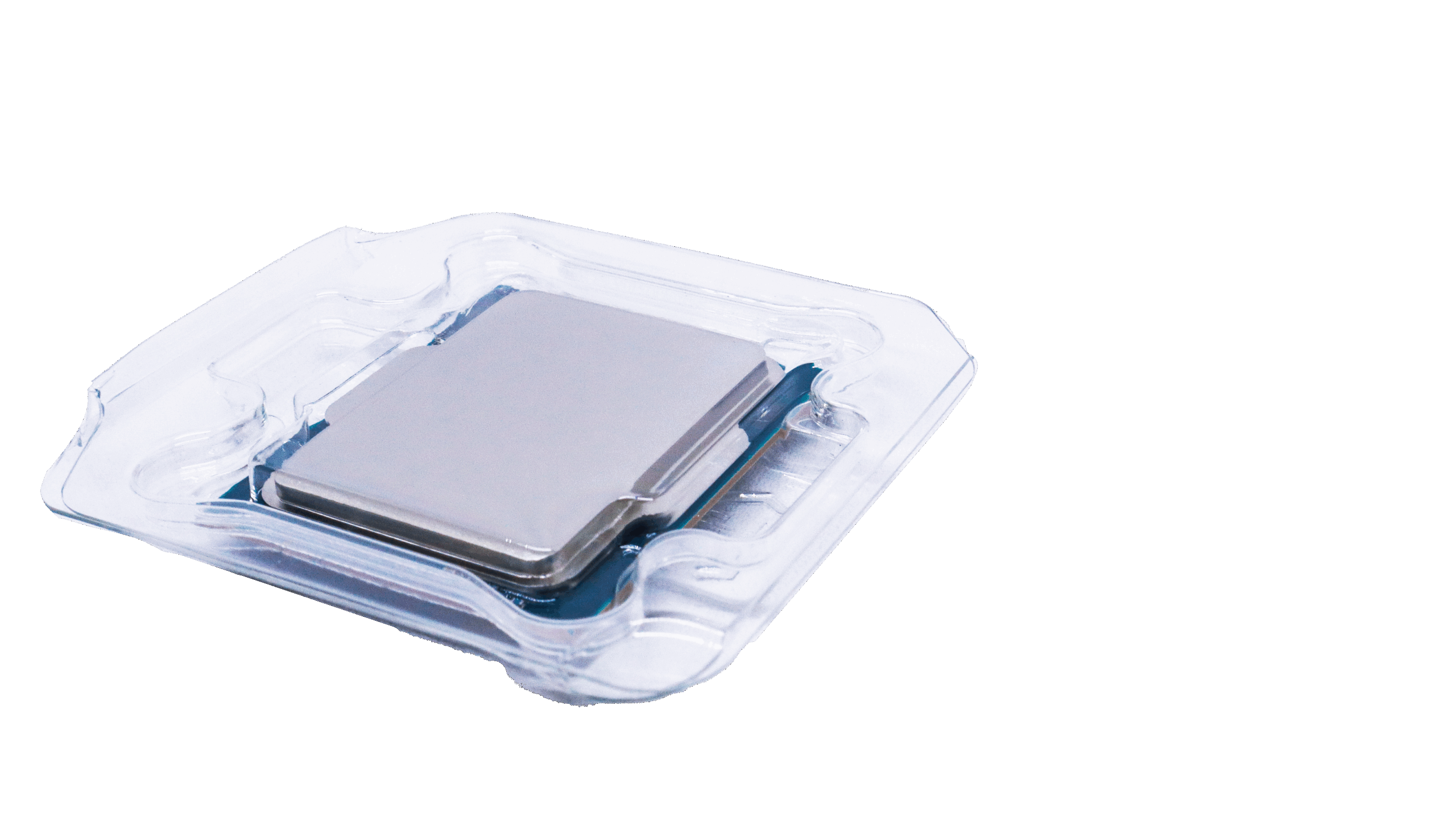
Impact and vibration: Delicate solder points, connectors, and screens need secure, form-fitting trays or clamshells to prevent shifting and damage during shipping or handling.
Environmental exposure: Moisture, dust, and debris can compromise product reliability. Consistent flange pressures and enclosed form-fit designs help maintain a clean, protective environment for components moving through production stages.
Weak points and touch areas: Buttons, ports, and corners require careful design consideration. Wall thickness, draw depths, and structural ribs are influenced by these features to maintain component integrity.
Defining protection requirements upfront ensures packaging is both manufacturable and performance-ready. It sets the foundation for a design that can move smoothly from prototype to production without unexpected failures.
Selecting the Right Materials for Electronic Packaging
Material choice is one of the most critical decisions when designing electronic packaging. The right resin provides static protection, formability, durability, and visual clarity while keeping production efficient and cost-effective.
When evaluating materials, engineers must consider how each option performs under real-world conditions. ESD-safe plastics are essential to dissipate static charge and protect sensitive electronics during handling, transport, and assembly. At Elmes, Electrostatic Dissipative (ESD) PET offers the right combination of safety and thermoforming reliability. Formability and durability are equally important: resins must maintain structural integrity during deep draws, flanges, and multi-pocket designs. Choosing a material that forms consistently helps prevent wall thinning, sticking, or blister separation. Clarity and visibility are also considerations. Depending on the product, materials can be transparent, translucent, or opaque to balance protective performance with product visibility.
By selecting the right ESD-safe, thermoformable material upfront, engineers create packaging that protects electronics, supports automated handling, and performs reliably through design validation and production scaling.
Designing Thermoformed Packaging for Electronics
Thermoformed electronic packaging must provide secure fit, manufacturability, and component protection. Pockets, flanges, and contours need to be engineered precisely to avoid production issues and maintain part integrity.
Critical design elements include:
Form-fit pocket geometry: Contoured pockets hold components securely in place, preventing movement during shipping, handling, or automated assembly. Depth, radius, and spacing all influence performance.
Flange width and tolerances: Consistent flange dimensions maintain reliable sealing and alignment. Tight tolerance control reduces the risk of blister separation or misaligned closures.
Material distribution and draw ratio: Ensuring even wall thickness and avoiding excessive thinning is essential for durability and consistent form. Female tooling can improve detail and definition in complex pockets.
Avoiding multi-plane cuts: Complicated edges and non-planar features can lead to inconsistent forming, difficult sealing, and higher scrap rates. Simplifying geometries early prevents production headaches.
Thoughtful attention to these design principles allows engineers to maximize product protection, streamline manufacturing, and reduce costly rework, creating packaging that performs reliably every step of the way.
Prototype Tooling and Production Considerations for Electronic Packaging
Prototyping is a crucial step in developing electronic packaging because it allows engineers to validate fit, flange tolerances, pocket geometry, and material behaviour before full-scale production. During prototype testing, components are placed in the form-fit pockets to confirm they remain secure, while flanges and seals are checked for proper alignment. This process ensures that minor adjustments—such as tweaks to draft angles, flange widths, or pocket depths—can be made early, reducing the risk of costly rework during production.
ESD-safe materials are evaluated in the prototype stage to verify consistent forming, wall thickness, and release characteristics. Any discrepancies between prototype and production materials can be identified and corrected, ensuring reliability and consistency throughout the process. By confirming that the final geometry can be manufactured at scale, prototyping helps guarantee that electronic packaging meets quality, performance, and cost targets.
Overall, prototype tooling is essential for reducing risk, validating design assumptions, and ensuring that the final packaging performs reliably throughout assembly, handling, and shipping.
Get Expert Help Designing Reliable Electronic Packaging
Effective electronic packaging begins with understanding your product’s protection requirements, selecting the right ESD-safe materials, and designing precise thermoformed pockets, flanges, and draft angles. Validating these decisions through prototyping ensures components remain secure and packaging forms consistently before full-scale production. Considering fulfillment and automation requirements during design further guarantees that packaging integrates smoothly into assembly, shipping, and handling processes.
At Elmes, our engineering-first approach supports you at every stage. From material selection and prototype tooling to production tooling and quality assurance, we help you create cost-effective, high-performing electronic packaging.
Contact us today to discuss your project or request a quote, and let our experts help you design electronic packaging that protects your products and integrates into your production process.